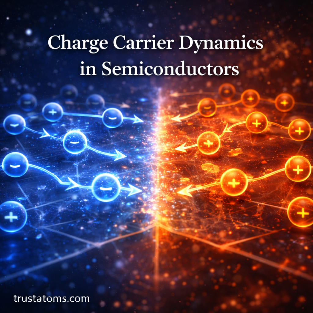
Every smartphone, computer chip, and solar panel depends on a deep principle in solid-state physics: charge carrier dynamics in semiconductors.
Unlike metals, where electrons flow freely, semiconductors carefully control how electric charge moves. The behavior of charge carriers — electrons and “holes” — determines how transistors switch, how LEDs emit light, and how solar cells generate electricity.
In this article, we’ll explore what charge carriers are, how they move, and why their dynamics are central to modern technology.
What Are Charge Carriers?
A charge carrier is any particle that carries electric charge through a material.
In semiconductors, there are two primary charge carriers:
- Electrons (negative charge)
- Holes (effective positive charge)
Electrons are real particles. Holes, however, are conceptual — they represent the absence of an electron in a crystal lattice.
When an electron leaves its position in the lattice:
- It creates an empty energy state.
- That empty state behaves like a positively charged particle.
- Nearby electrons can move into the vacancy.
- The hole appears to move in the opposite direction.
This dual-carrier system is what makes semiconductors unique.
Energy Bands and Carrier Formation
To understand charge carrier dynamics, we need to look at energy bands.
In solids:
- The valence band contains electrons bound to atoms.
- The conduction band contains free-moving electrons.
- The band gap separates the two.
In semiconductors:
- The band gap is small.
- Thermal energy can excite electrons into the conduction band.
- When electrons jump to the conduction band, holes form in the valence band.
This excitation process creates mobile charge carriers.
Intrinsic vs. Extrinsic Semiconductors

Charge carrier behavior depends on the type of semiconductor.
Intrinsic Semiconductors
- Pure material (like silicon).
- Equal number of electrons and holes.
- Conductivity depends on temperature.
As temperature increases:
- More electrons cross the band gap.
- Carrier concentration increases.
- Conductivity rises.
Extrinsic Semiconductors
Doping introduces impurity atoms to control carrier concentration.
There are two main types:
- n-type semiconductor
- Doped with atoms that donate extra electrons.
- Electrons are the majority carriers.
- p-type semiconductor
- Doped with atoms that create holes.
- Holes are the majority carriers.
Doping allows precise control over electrical properties.
Drift and Diffusion: Two Modes of Carrier Motion
Charge carriers move in two primary ways: drift and diffusion.
Drift Current
Drift occurs when an external electric field is applied.
- Electrons move opposite the electric field.
- Holes move in the same direction as the field.
- The stronger the field, the faster the drift velocity.
Drift current is responsible for transistor operation and circuit functionality.
Diffusion Current
Diffusion occurs due to concentration differences.
- Carriers move from high concentration to low concentration.
- No external electric field is required.
- Movement continues until equilibrium is reached.
Diffusion is critical in p–n junctions and diode behavior.
Mobility and Conductivity
Carrier mobility describes how quickly a charge carrier moves under an electric field.
Mobility depends on:
- Lattice structure
- Temperature
- Impurities
- Scattering events
Higher mobility means:
- Faster electronic switching
- Lower resistance
- Better device performance
Electrical conductivity in semiconductors depends on:
- Carrier concentration
- Carrier mobility
Both must be optimized for high-performance devices.
Recombination and Generation
Charge carriers are not permanent.
Two key processes constantly occur:
Generation
- Thermal energy excites electrons.
- Electron–hole pairs are created.
- Carrier concentration increases.
Recombination
- An electron falls back into a hole.
- Energy is released.
- Carrier concentration decreases.
The balance between generation and recombination determines steady-state carrier levels.
In LEDs, recombination releases light.
In solar cells, generation from sunlight creates usable current.
Charge Carrier Dynamics in p–n Junctions
The p–n junction is the foundation of semiconductor devices.
When p-type and n-type materials meet:
- Electrons diffuse into the p-region.
- Holes diffuse into the n-region.
- A depletion region forms.
- An internal electric field develops.
This built-in field controls carrier movement.
Under forward bias:
- Carriers cross the junction easily.
- Current flows.
Under reverse bias:
- Carrier movement is restricted.
- Current is minimal.
This behavior enables diodes, transistors, and integrated circuits.
Carrier Lifetime and Device Performance
Carrier lifetime refers to how long a charge carrier exists before recombination.
Longer lifetimes are important for:
- Solar cells (maximize current output)
- Photodetectors
- Power electronics
Short lifetimes are desirable in:
- High-speed switching devices
- Certain logic circuits
Engineers tailor carrier lifetime through material design and doping control.
Temperature Effects on Carrier Dynamics
Temperature strongly influences semiconductor behavior.
As temperature rises:
- Carrier generation increases.
- Mobility decreases due to increased lattice vibrations.
- Overall conductivity changes.
At very high temperatures, excessive carrier generation can disrupt device performance.
Thermal management is therefore critical in microelectronics.
Why Charge Carrier Dynamics Matter
Modern electronics depend entirely on controlling charge carrier movement.
Understanding carrier dynamics enables:
- Faster processors
- Efficient solar panels
- Bright and energy-efficient LEDs
- Sensitive photodetectors
- Advanced communication systems
Every transistor in a microchip operates by manipulating electron and hole motion.
Without precise control over carrier dynamics, integrated circuits would not function.
The Future of Semiconductor Carrier Research
Emerging materials like:
- Gallium nitride
- Silicon carbide
- Two-dimensional materials (such as graphene derivatives)
are pushing the boundaries of carrier mobility and performance.
Researchers are exploring:
- Ultra-fast carrier transport
- Reduced scattering effects
- Quantum transport phenomena
- Nanoscale device architectures
As device dimensions shrink, understanding carrier dynamics at quantum scales becomes increasingly important.
Final Thoughts
Charge carrier dynamics in semiconductors explain how electrons and holes move, interact, and respond to electric fields inside materials.
Through processes like drift, diffusion, generation, and recombination, semiconductors enable the precise control of electrical signals.
From smartphones to solar panels, nearly every modern electronic system relies on these fundamental physical principles.
Mastering charge carrier behavior isn’t just theoretical physics — it’s the engine behind the digital world.