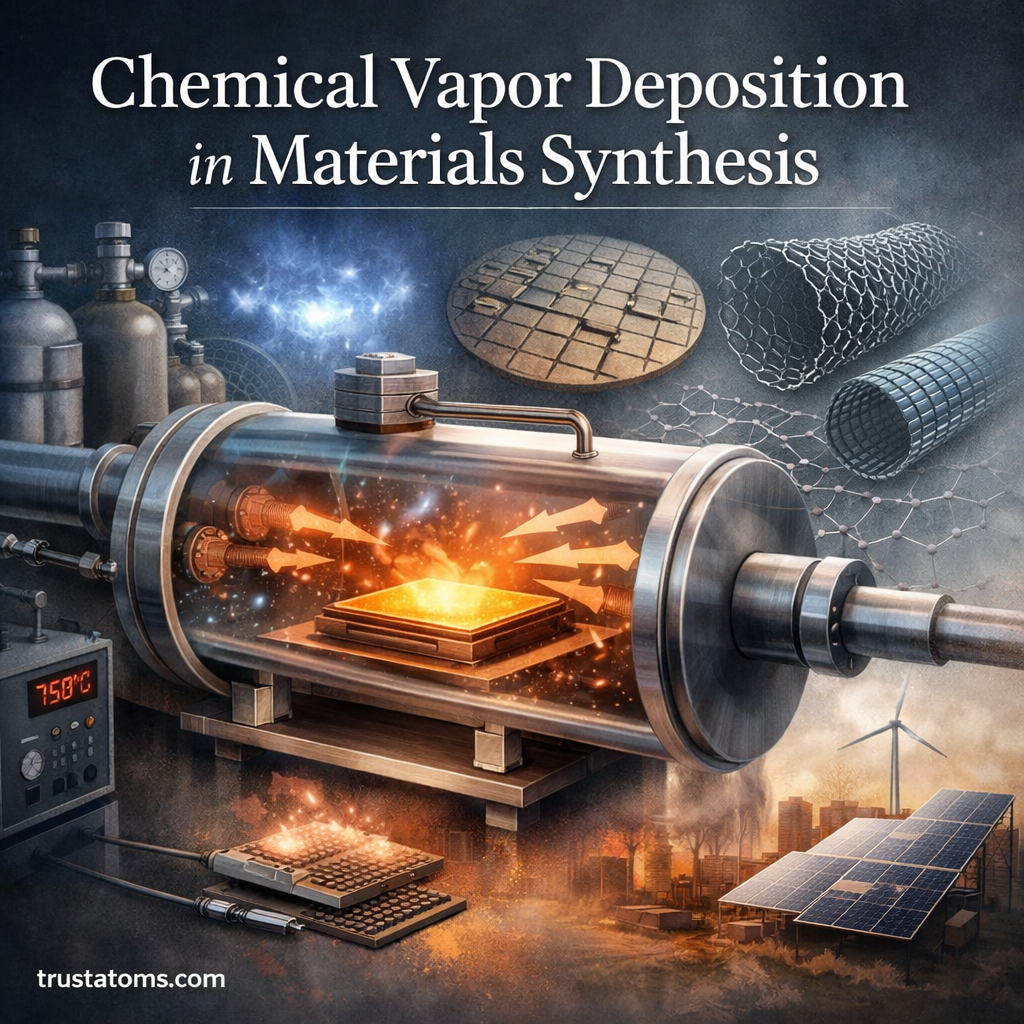
Chemical Vapor Deposition (CVD) is one of the most important techniques used in modern materials science. It enables scientists and engineers to create extremely thin, high-quality material layers on a surface by using chemical reactions in the vapor phase.
This process plays a crucial role in industries such as semiconductor manufacturing, nanotechnology, coatings, and advanced materials engineering. From computer chips to protective coatings and graphene production, CVD allows precise control over how materials form at the microscopic level.
Understanding how Chemical Vapor Deposition works helps explain how many of the high-performance materials in electronics, aerospace, and energy technologies are created.
What Is Chemical Vapor Deposition?
Chemical Vapor Deposition is a materials synthesis method where gaseous chemicals react or decompose on a heated surface to form a solid material layer.
During the process:
- A substrate (the surface to coat) is placed inside a reaction chamber.
- Reactive gases are introduced into the chamber.
- Heat or energy causes chemical reactions to occur.
- A thin solid film forms on the substrate surface.
The resulting layer can range from a few atoms thick to several micrometers depending on the process conditions.
This technique is valued because it can produce extremely uniform, pure, and precisely controlled material films.
How the CVD Process Works
Although there are many variations, the general steps of Chemical Vapor Deposition follow a similar sequence.
1. Introduction of Reactive Gases
Special precursor gases containing the desired elements are pumped into the reaction chamber.
Examples include gases containing:
- Silicon
- Carbon
- Titanium
- Tungsten
These gases serve as the chemical source for the material that will be deposited.
2. Gas Transport and Diffusion
The gases move through the chamber and diffuse toward the substrate surface. Controlled temperature, pressure, and flow rates help ensure uniform coverage.
3. Chemical Reaction at the Surface
When the gas molecules reach the heated substrate, they undergo chemical reactions such as:
- Thermal decomposition
- Chemical reduction
- Surface reactions between gases
These reactions produce a solid material that bonds to the substrate.
4. Film Formation
Atoms or molecules accumulate on the surface and gradually form a thin, continuous film. The thickness and structure of the film depend on factors like temperature, gas composition, and deposition time.
5. Removal of Byproducts
Unused gases and reaction byproducts are carried away by the gas flow and removed from the chamber.
Types of Chemical Vapor Deposition
Different forms of CVD are used depending on the application and required material properties.
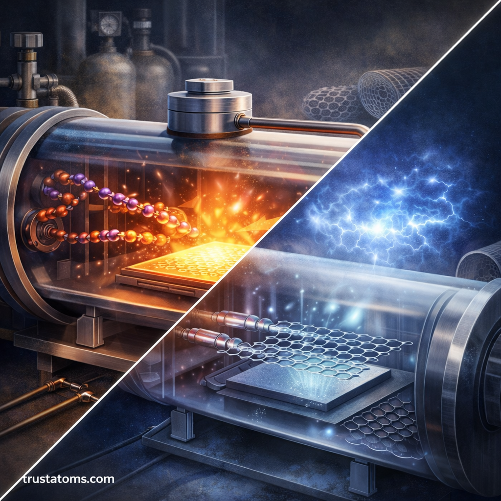
Thermal CVD
Thermal CVD relies primarily on high temperatures to drive chemical reactions.
Common features include:
- Temperatures often between 600°C and 1200°C
- Used for silicon, tungsten, and diamond coatings
- Widely applied in semiconductor fabrication
Plasma-Enhanced CVD (PECVD)
Plasma-Enhanced Chemical Vapor Deposition uses plasma energy to activate chemical reactions.
Advantages include:
- Lower processing temperatures
- Faster reaction rates
- Suitable for temperature-sensitive substrates
PECVD is often used to deposit materials on glass, polymers, or delicate electronic components.
Low-Pressure CVD (LPCVD)
Low-Pressure CVD operates at reduced pressure to improve film uniformity and reduce unwanted reactions.
Benefits include:
- High-quality films
- Excellent step coverage
- Good uniformity across large surfaces
Metal-Organic CVD (MOCVD)
MOCVD uses metal-organic precursor molecules to deposit complex materials, especially semiconductor compounds.
It is commonly used for producing:
- LED materials
- Advanced semiconductor structures
- Optoelectronic components
Materials Produced Using CVD
Chemical Vapor Deposition is capable of producing a wide range of advanced materials.
Common examples include:
- Silicon thin films for computer chips
- Diamond coatings for cutting tools
- Carbon nanotubes
- Graphene sheets
- Titanium nitride protective coatings
- Ceramic layers for high-temperature components
These materials often have superior purity and structural control compared to many other synthesis techniques.
Advantages of Chemical Vapor Deposition
CVD has become a cornerstone of advanced manufacturing because of several key benefits.
High Purity Materials
The chemical reactions involved in CVD can produce extremely pure materials with minimal contamination.
Uniform Thin Films
CVD can coat surfaces evenly, even on complex shapes and microscopic features.
Excellent Adhesion
The deposited film forms strong bonds with the substrate, resulting in durable coatings.
Precise Thickness Control
Engineers can carefully control deposition time, temperature, and gas flow to achieve very specific film thicknesses.
Challenges and Limitations
Despite its advantages, Chemical Vapor Deposition also has some challenges.
High Equipment Costs
CVD systems require specialized reactors, gas delivery systems, and safety controls.
High Temperatures
Some processes require very high temperatures, which may limit compatible materials.
Toxic or Reactive Gases
Certain precursor chemicals used in CVD can be hazardous and require strict safety protocols.
Process Complexity
Precise control of temperature, pressure, and gas flow is essential for consistent results.
Applications of CVD in Modern Technology
Chemical Vapor Deposition supports many technologies used in everyday life and advanced research.
Semiconductor Manufacturing
CVD is essential for building microelectronic components such as:
- Transistors
- Integrated circuits
- Memory chips
Thin films created through CVD form insulating layers, conductive pathways, and semiconductor structures.
Protective Coatings
CVD coatings improve durability and resistance to wear and corrosion.
Examples include:
- Cutting tool coatings
- Turbine blade protection
- Hard coatings for industrial components
Nanotechnology and Advanced Materials
CVD enables the synthesis of nanomaterials like:
- Graphene
- Carbon nanotubes
- Nanowires
These materials are used in electronics, sensors, energy storage, and advanced composites.
Renewable Energy
Solar cells and battery technologies often rely on thin films produced through Chemical Vapor Deposition to improve efficiency and durability.
Why Chemical Vapor Deposition Matters in Materials Science
Chemical Vapor Deposition allows scientists to build materials with atomic-level precision. This capability has transformed industries ranging from computing and aerospace to energy and medicine.
As technology continues to advance, the demand for thinner, stronger, and more precise materials will continue to grow. CVD remains one of the most powerful tools available for synthesizing those materials.
By enabling controlled growth of high-performance films and nanostructures, Chemical Vapor Deposition plays a central role in shaping the materials that power modern innovation.
Related Posts
 What Is a Redox Reaction?
 What Is a Solute?
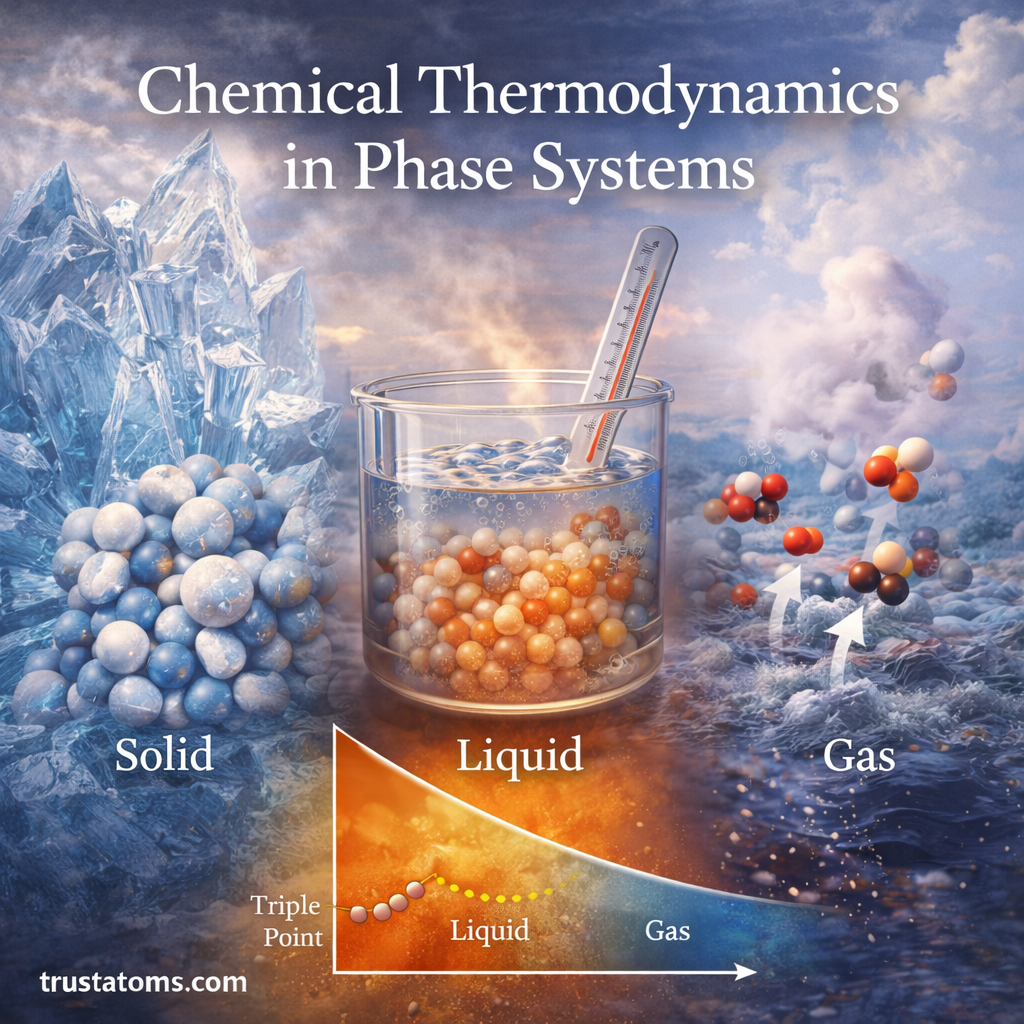 Chemical Thermodynamics in Phase Systems
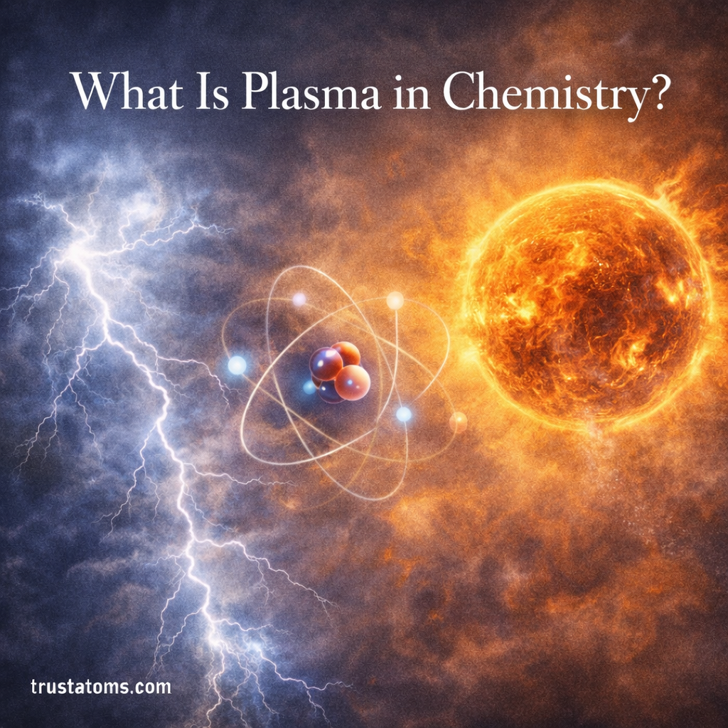 What Is Plasma in Chemistry?