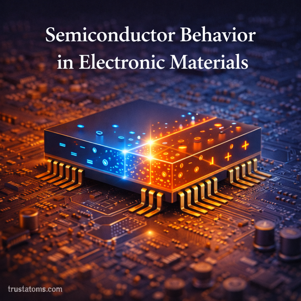
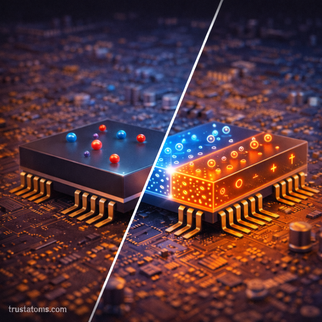
Semiconductors are the foundation of modern technology. From smartphones and computers to solar panels and advanced medical devices, semiconductor materials make electronic control possible.
But what exactly is semiconductor behavior? How can a material sometimes conduct electricity and sometimes resist it?
In this guide, we’ll explore the physics behind semiconductor behavior, how electrons move in these materials, and why semiconductors are essential in electronic systems.
What Is a Semiconductor?
A semiconductor is a material with electrical conductivity between that of a conductor and an insulator.
- Conductors (like copper) allow electrons to flow easily.
- Insulators (like rubber) strongly resist electron flow.
- Semiconductors fall in between.
The most common semiconductor material is silicon, though others like germanium and gallium arsenide are also widely used.
What makes semiconductors unique is that their conductivity can be controlled.
Atomic Structure and Energy Bands
To understand semiconductor behavior, we need to examine electron energy levels.
Energy Bands
In solid materials, electrons do not occupy isolated energy levels. Instead, they form energy bands:
- Valence band – where electrons are normally bound to atoms
- Conduction band – where electrons are free to move and conduct electricity
- Band gap – the energy gap between the valence and conduction bands
The size of the band gap determines whether a material behaves as:
- A conductor (small or overlapping bands)
- An insulator (large band gap)
- A semiconductor (moderate band gap)
Semiconductors have a band gap small enough that electrons can be excited into the conduction band under certain conditions.
Intrinsic Semiconductors
An intrinsic semiconductor is a pure semiconductor material without added impurities.
At low temperatures:
- Most electrons remain in the valence band.
- Very little current flows.
As temperature increases:
- Thermal energy excites electrons.
- Some electrons jump to the conduction band.
- This leaves behind “holes” in the valence band.
- Both electrons and holes can carry charge.
This dual charge-carrier behavior is a key property of semiconductors.
Electrons and Holes
In semiconductors, current flows through two types of charge carriers:
- Electrons (negative charge)
- Holes (positive charge)
What Is a Hole?
When an electron leaves the valence band:
- It creates a vacancy.
- Nearby electrons move to fill the gap.
- The vacancy appears to move in the opposite direction.
This moving vacancy is called a hole.
Both electrons and holes contribute to electrical conduction.
Doping: Controlling Conductivity
Pure semiconductors have limited conductivity. To enhance their behavior, impurities are intentionally added. This process is called doping.
n-Type Semiconductors
If atoms with extra electrons are added:
- Extra free electrons become available.
- Electrons are the majority carriers.
These materials are called n-type (negative-type).
p-Type Semiconductors
If atoms with fewer valence electrons are added:
- Additional holes are created.
- Holes become the majority carriers.
These materials are called p-type (positive-type).
Doping allows engineers to precisely control electrical properties.
The p-n Junction
When p-type and n-type materials are joined, a p-n junction forms.
This junction is the basis of:
- Diodes
- Transistors
- Solar cells
- LEDs
What Happens at the Junction?
- Electrons diffuse from n-type to p-type.
- Holes diffuse from p-type to n-type.
- A depletion region forms.
- An internal electric field develops.
This electric field controls current flow, allowing the junction to act as an electrical switch.
Semiconductor Behavior in Electric Fields
When voltage is applied across a semiconductor device:
- Charge carriers respond to the electric field.
- Current flow can increase or decrease depending on direction.
In a diode:
- Forward bias reduces the barrier and allows current.
- Reverse bias increases the barrier and blocks current.
This directional behavior is essential in electronic circuits.
Temperature Effects on Semiconductor Behavior
Unlike conductors, semiconductor conductivity increases with temperature.
Why?
- Higher temperature excites more electrons.
- More electrons enter the conduction band.
- More holes are created.
- Overall conductivity rises.
This temperature sensitivity is important in sensor applications.
Semiconductor Devices in Electronics
Semiconductor behavior enables nearly all modern electronic devices.
Diodes
- Allow current in one direction.
- Used in rectifiers and signal processing.
Transistors
- Act as switches or amplifiers.
- Form the building blocks of integrated circuits.
Integrated Circuits (ICs)
- Contain millions or billions of transistors.
- Enable processors, memory chips, and microcontrollers.
Solar Cells
- Convert light energy into electrical energy.
- Rely on p-n junction physics.
Advantages of Semiconductor Materials
Semiconductors provide:
- Controlled conductivity
- Switching capability
- Amplification properties
- Miniaturization potential
- Energy-efficient operation
Their tunable behavior makes them more versatile than simple conductors.
Limitations and Challenges
Despite their advantages, semiconductors have constraints:
- Sensitive to temperature changes
- Manufacturing complexity
- Material defects can affect performance
- Limited performance at extremely high temperatures
Engineers carefully design devices to manage these limitations.
Why Semiconductor Behavior Matters
Understanding semiconductor behavior explains how:
- Smartphones process data
- Computers store information
- Power electronics regulate voltage
- Renewable energy systems generate electricity
- Communication systems transmit signals
Modern digital society depends entirely on controlled semiconductor behavior.
Final Thoughts
Semiconductor behavior in electronic materials is one of the most transformative discoveries in physics and engineering.
By controlling how electrons and holes move through materials, scientists and engineers have built the foundation of modern electronics. From simple diodes to advanced microprocessors, semiconductors make precise electrical control possible.
Understanding how energy bands, doping, and charge carriers interact gives you insight into the invisible processes powering today’s technology.